A small hole in a PCB pad can change what happens to the solder during reflow. Even when there appears to be plenty of solder paste on the pad, some of that solder may end up inside the via rather than around the component termination.
An experiment shared on Reddit provides a particularly clear example. It also raises a question that deserves a more careful answer than simply saying that via-in-pad is bad design: when does an open via create an assembly problem, and when is placing a via inside a pad a reasonable engineering choice?
A Reflow Experiment With 0603 Components
In March 2025, a contributor to r/PrintedCircuitBoard shared photographs from a reflow experiment involving a PCB originally designed for hand soldering.
The contributor had recently completed a Controleo3 reflow oven build and was using spare boards with 0603 components to test the oven. Two of the component pads contained open vias. The via holes were 0.3 mm in diameter, a size selected partly to keep the original board fabrication inexpensive.
The test was intended to make a known soldering risk visible.
Despite depositing a generous amount of solder paste, the contributor observed that the joints associated with the open vias had substantially less solder remaining after reflow.
This was an informal demonstration, not a production failure report or a controlled study. The board had originally been designed for hand soldering. Even so, the photographs clearly show how molten solder can move around an open via.
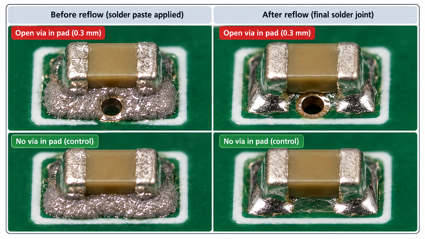
Where Did the Solder Go?
The mechanism is solder wicking.
When solder paste is heated beyond its melting range during reflow, the molten solder wets the available solderable surfaces. If a plated through-hole via is open inside the component pad, it introduces an additional path into which the solder can flow.
The metal-lined via barrel can draw solder away from the surface pad. Depending on the geometry of the hole and the amount of available solder, this can leave less material at the component termination than the joint was designed to receive.
Texas Instruments describes this issue in its application report SNVA839, explaining that vias located inside component pads can reduce solder coverage and potentially compromise thermal or electrical performance.
The visible result is not necessarily the same for every PCB. Hole diameter, board thickness, solder volume, surface finish, pad geometry, and the thermal behavior of the assembly all matter.
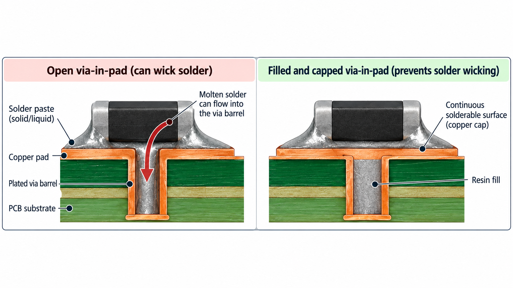
In the open-via example, the solderable barrel remains accessible from the pad surface. In the filled-and-capped example, the pad has a continuous copper-covered surface, preventing molten solder from draining into the via barrel through the pad opening.
What matters, then, is the via construction, not simply whether a via sits beneath the component.
What the Reddit Experiment Shows, and What It Does Not
The Reddit discussion was not entirely in agreement about the interpretation of the photographs.
Some commenters pointed to the open vias as the expected cause of solder loss. Others questioned whether the reflow process itself had reached an appropriate thermal profile, noting that the appearance of some solder joints suggested insufficient heating or incomplete reflow.
Both explanations can be valid.
An open via can create a path for solder loss, while an unsuitable reflow profile can independently affect solder wetting and the final appearance of a joint. A photograph alone does not establish how much each factor contributed.
The experiment also did not include controlled comparisons across different via diameters, board thicknesses, or solder paste deposition volumes.
The test shows a credible failure mechanism, but it does not establish failure rates or prove that every open via-in-pad layout will behave the same way.
That limit should remain clear when turning a workshop demonstration into design guidance.
Why Smaller Vias May Help
Several participants in the Reddit discussion suggested that smaller via holes could reduce solder loss. Some described successful prototype assemblies using hole diameters around 0.15 or 0.2 mm.
A smaller opening changes both the geometry and the volume available for solder to enter.
Texas Instruments similarly notes that using smaller finished holes can help limit solder wicking.
However, a smaller open via is not equivalent to a filled and capped via.
Its behavior still depends on the full pad-and-via structure: barrel geometry, board thickness, stencil deposit, and assembly process. A hole size that works in one design is not a universal rule for the next.
Smaller mechanical drills or microvia processes may also introduce their own manufacturing capabilities and cost constraints.
Filled and Capped Vias: A Different Structure
When a via must be placed directly inside a solderable pad, a filled-and-capped construction can remove the open path into the via barrel.
In a typical via-in-pad plated-over process, the plated via is filled with a suitable material, planarized, and covered with copper plating to restore a continuous pad surface.
This approach is particularly relevant to high-density layouts in which there is insufficient space to move a via away from the component pad.
It may also be necessary where short connections are important to the electrical layout, such as certain BGA fanouts and dense component placements.
The tradeoff is that filling and capping require additional PCB fabrication operations. Design requirements should therefore specify the intended via treatment rather than using terms such as tented, plugged, filled, and plated over interchangeably.
Tenting an open via with solder mask is another technique sometimes used to limit solder movement. However, it does not produce the same structure as a filled and copper-capped via. Depending on which side is covered and how gases behave during reflow, different voiding or assembly risks may arise.
The QFN Exception: Thermal Vias Are Not Automatically Mistakes
A large exposed thermal pad changes the design problem.
Many QFN packages use thermal vias to conduct heat from the exposed pad into internal or opposite-side copper planes.
Removing all those vias merely to avoid solder wicking could compromise the thermal intent of the layout.
Texas Instruments addresses this tradeoff in its Array QFN Application Note, SLMA006. The document discusses thermal vias, solder loss, via plugging, and solder-mask tenting for a specific QFN design. It also provides an example using 0.3 mm drill diameters to help control solder loss.
A 0.3 mm opening is not suitable for every component. The acceptable via construction depends on the package and its soldering geometry.
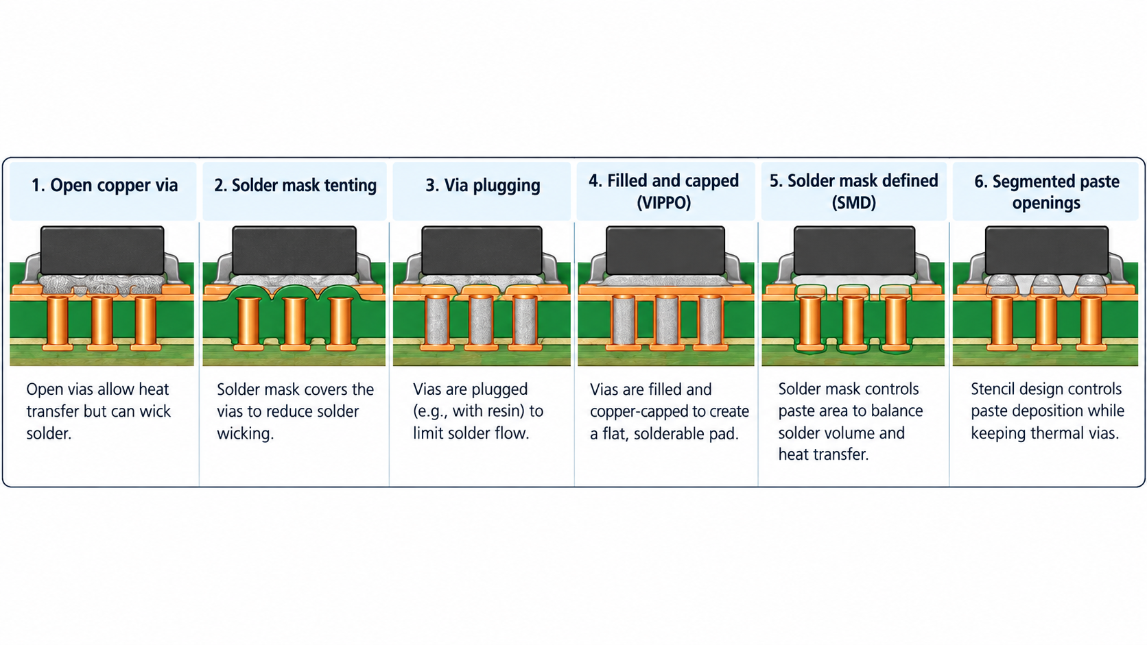
A separate engineering study, published in Circuits Assembly, compared alternative via and solder-mask arrangements for bottom-terminated components. Its proposed design uses conventional through-hole vias together with controlled solder-mask openings and stencil patterns.
The study does not make filled-and-capped vias unnecessary. It shows that via placement, solder-mask geometry, paste deposition, thermal performance, and manufacturability have to be evaluated together.
What to Check Before Releasing the PCB Layout
For small passive components, an open through-hole via directly inside a solder pad deserves particular attention. Where routing space permits, relocating the via away from the solderable area avoids creating that particular path for solder loss.
When the via cannot be moved, the question becomes whether the intended fabrication process can provide a suitable filled, capped, or otherwise controlled via structure.
For QFN exposed pads and similar thermal features, the manufacturer's recommended land pattern and assembly guidance should be the starting point. The via arrangement must accommodate heat transfer as well as solder joint formation.
Stencil openings also matter. More paste does not correct an uncontrolled open-via geometry. The deposited solder volume and the available wetting surfaces must suit the intended joint.
During prototype evaluation, photographs can reveal visible soldering problems, but they may not show hidden defects beneath a package. When those connections are critical, an appropriate inspection method, potentially including X-ray imaging, may be required.
The specific acceptance criteria depend on the component and applicable assembly requirements.
A Design Choice, Not a Blanket Rule
The Reddit experiment is not an argument against every via-in-pad design.
It shows that an exposed via barrel inside a solderable pad changes the path available to molten solder. The risk depends on the geometry and process, so it belongs in the layout review before fabrication.
The demonstration makes the problem visible. Manufacturing literature explains the mechanism, while component application notes show why some packages still require vias inside their pads.
Via-in-pad is neither universally good nor universally bad. Its construction has to match the component, the thermal requirement, and the assembly process.